

Summary
- Infineon plans approximately €1.1bn of investment in Villach by 2034.
- The project would move 300mm gallium nitride power semiconductors into high-volume production from late 2027.
- The Commission approved €319m of state aid, but Austria's formal funding commitment remains outstanding.
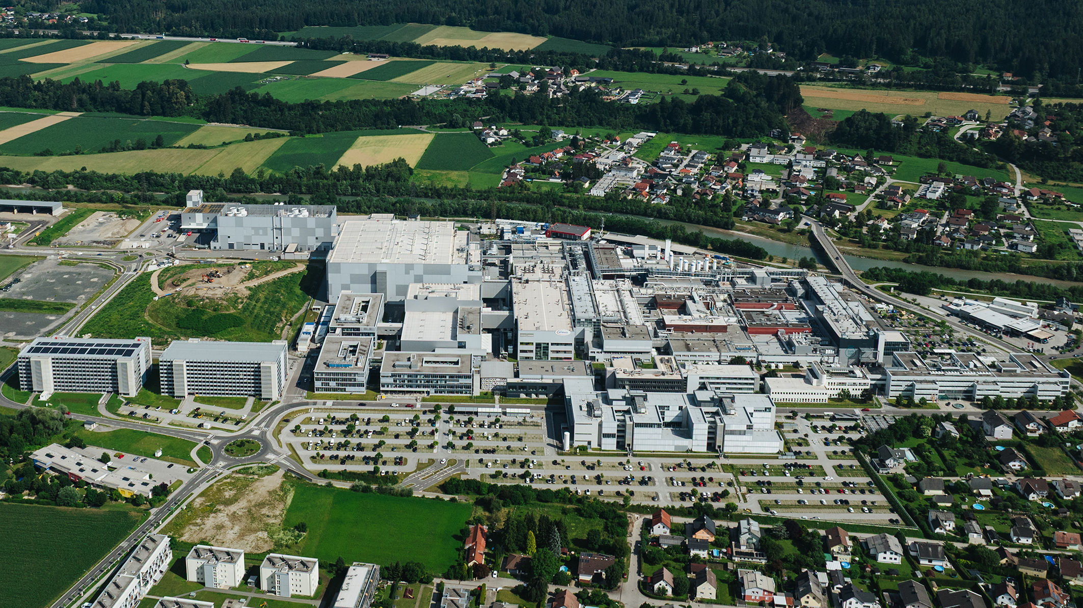
Infineon Technologies plans to invest about €1.1bn in its Villach semiconductor operation in Austria, moving gallium nitride power-chip production on 300mm wafers towards industrial scale. The company expects production to begin by the end of 2027, while its investment programme extends to 2034.
The European Commission has approved €319m of proposed Austrian state aid under the European Chips Act. However, the Federal Ministry for Economic Affairs, Energy and Tourism must still issue its formal funding commitment. Approval of a state-aid measure is not evidence that the money has already been disbursed.
Gallium nitride, commonly abbreviated to GaN, supports high-frequency power switching and efficient electricity conversion. Its applications include power supplies for AI facilities, energy infrastructure, vehicle charging and industrial equipment, where conversion losses and heat affect operating costs.
The devices do not perform AI calculations. Their value lies in providing and controlling electrical power for processors and other systems, making them part of the supporting infrastructure rather than a substitute for advanced computing chips.
Larger wafers, but not guaranteed yields
Infineon demonstrated processing 300mm GaN wafers two years ago. A 300mm wafer has 2.25 times the surface area of a 200mm wafer, while the company estimates the larger format can yield around 2.3 times as many chips per wafer.
That theoretical increase in chip count must be separated from saleable output. Defects, die yield, substrate quality, cycle times, equipment availability and test failures all affect the number of devices that meet customer requirements.
A larger wafer is commercially attractive because more devices can be processed in each production cycle. Yet the cost per working device also depends on equipment capital costs, materials, staff expertise and the throughput achieved over a sustained period.
Moving a process from a demonstration into high-volume manufacture adds technical challenges. Engineers must maintain consistent electrical properties and physical dimensions across large numbers of wafers, while customers may require lengthy qualification before changing supply arrangements.
Infineon says the manufacturing ramp-up will follow demand. The intended production start therefore does not mean the plant will operate at its ultimate capacity from day one, or that all customers will immediately switch to the new format.
An established Austrian industrial base
The company intends to use existing cleanroom space and upgraded facilities in Villach instead of constructing an entirely independent manufacturing campus. That approach may reduce some development barriers, although installation and production qualification still involve significant work.
Infineon reported approximately 4,800 employees at Villach at the end of the 2025 financial year, within an Austrian workforce of around 5,800. Research and production operations already located there provide a base for extending the process.
The location also connects manufacturing with local universities, researchers and specialist suppliers. Such relationships can be useful for technical recruitment and process development, but their existence does not establish the total economic impact of the new facility.
European semiconductor policy has concentrated on strengthening strategic capacity and reducing vulnerability to disruptions elsewhere. Advanced power electronics offer a different industrial opportunity from the most advanced processors used for AI inference and training.
Locating fabrication in the EU can broaden manufacturing options without making the supply chain entirely European. Equipment, wafer materials, packaging services and customers may still depend on international partners and cross-border logistics.
Funding conditions and the market test
Austria’s proposed support has secured European Commission approval, but the domestic ministry’s formal commitment is still awaited. The timing and conditions of payment will matter to an assessment of how much public finance ultimately supports the project.
The project also depends on customers adopting the resulting chips. Engineers designing power converters weigh efficiency against price, reliability, cooling requirements and the availability of qualified components, sometimes requiring changes to the broader circuit rather than a direct substitution.
Demand may develop differently across data centres, automotive products and electricity infrastructure. Each sector has distinct product lifetimes and qualification standards, so announced manufacturing capacity cannot be equated with immediately accessible sales.
Earlier in October, Infineon expanded its supply of silicon carbide wafers through an agreement with Wolfspeed, as Techopia reported. Silicon carbide and gallium nitride have different strengths in power electronics and their respective investments should not be conflated.
Infineon’s 27 October announcement documents the manufacturing plan, conditional state funding and production target. Realised yields, customer qualification and the performance of the resulting devices will determine the outcome beyond the investment commitment.
Public assistance can be justified by expected technological spillovers, including research collaboration and skills development, but those benefits must be assessed against actual delivery. The state-aid approval establishes the legal permissibility of the proposed support rather than measuring future regional productivity.
Greater GaN availability could also influence downstream equipment designers by reducing concerns about supply continuity. Those design decisions will still rely on verified electrical performance, product support and stable long-term component availability, not only on a manufacturer’s capital expenditure.
Scaling a new wafer format can require changes in handling, process control and inspection. Even where the semiconductor’s properties are well understood, industrialising a larger substrate means learning which production steps determine defect rates and whether that performance remains reproducible over time.


